PDF) Complete PCB Design Using OrCad Capture and Layout
Por um escritor misterioso
Last updated 10 abril 2025

is a platform for academics to share research papers.

How to Configure and Export a Smart PDF in OrCAD Capture
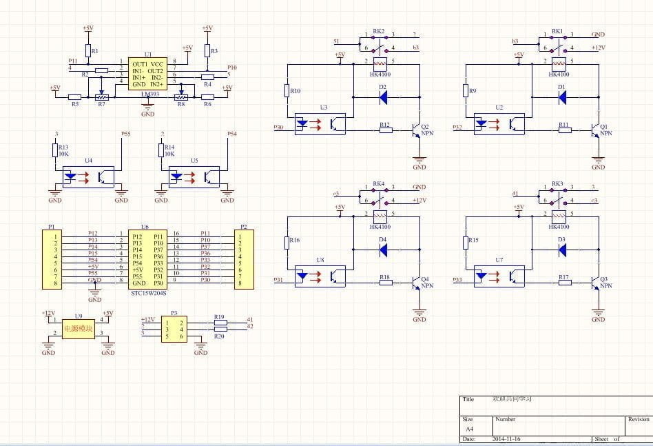
PCB Schematic Design - Step by Step Guide
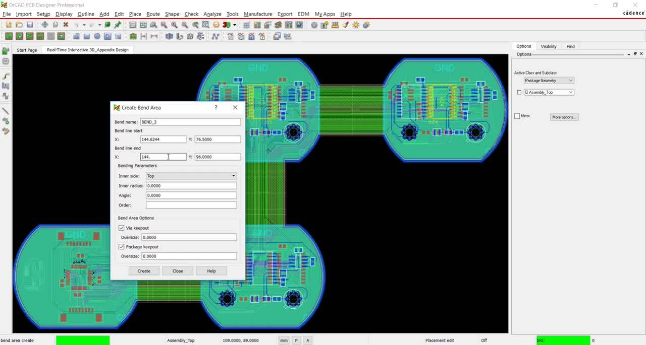
OrCAD PCB Designer Suite
OrCAD Version History EMA Design Automation

Complete PCB Design Using OrCAD Capture and PCB Editor: Mitzner

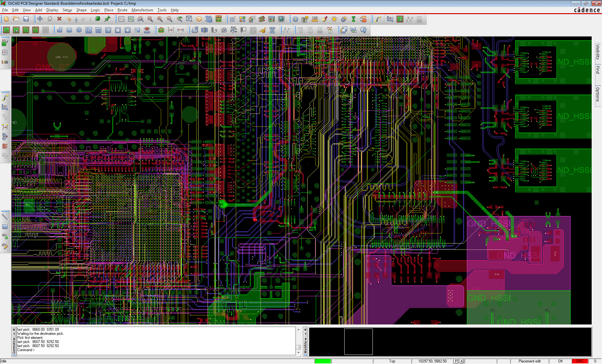
OrCAD Layout 17.2 Useful Tips
The top EDA tools for circuit and PCB design in 2023

Online Course: Learning PCB Design with OrCAD from LinkedIn

Pspice Simulation Profile - an overview
OrCAD Capture and PCB Editor Tutorials
OrCAD Tutorial Physical Layout - Parallel Systems
Recomendado para você
-
 BLOG - SMBOT10 abril 2025
 -
Grupo AutoRede10 abril 2025
-
 Hmong English Bilingualism10 abril 2025
Hmong English Bilingualism10 abril 2025 -
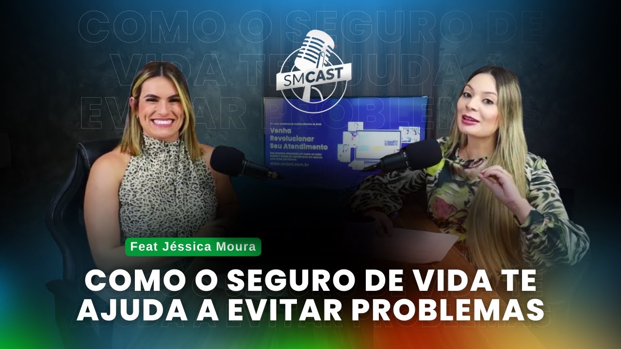 SMCAST - Jéssica Moura - Especialista em seguro de vida10 abril 2025
 -
SMCAST10 abril 2025
-
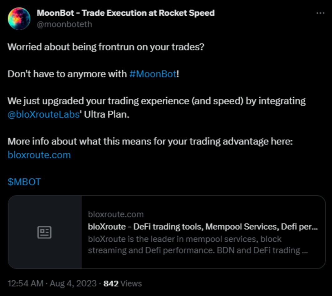 Curtis Plot Mak (@curtisplot) / X10 abril 2025
 -
6RL - 6ral Series10 abril 2025
-
Filipe Almeida 🏳️🌈 - Apresentador Apcap da Sorte - Apcap da Sorte10 abril 2025
-
 Chatbot para atendimento: vale a pena investir em um?10 abril 2025
 -
13 Jan 1875 - TOPICS OF THE DAY. - Trove10 abril 2025


você pode gostar
-
 ➥Obito Uchiha ▻ Naruto Amino10 abril 2025
 -
 Building : Part 1 - Getting Started10 abril 2025
 -
 Kleki designs, themes, templates and downloadable graphic elements10 abril 2025
 -
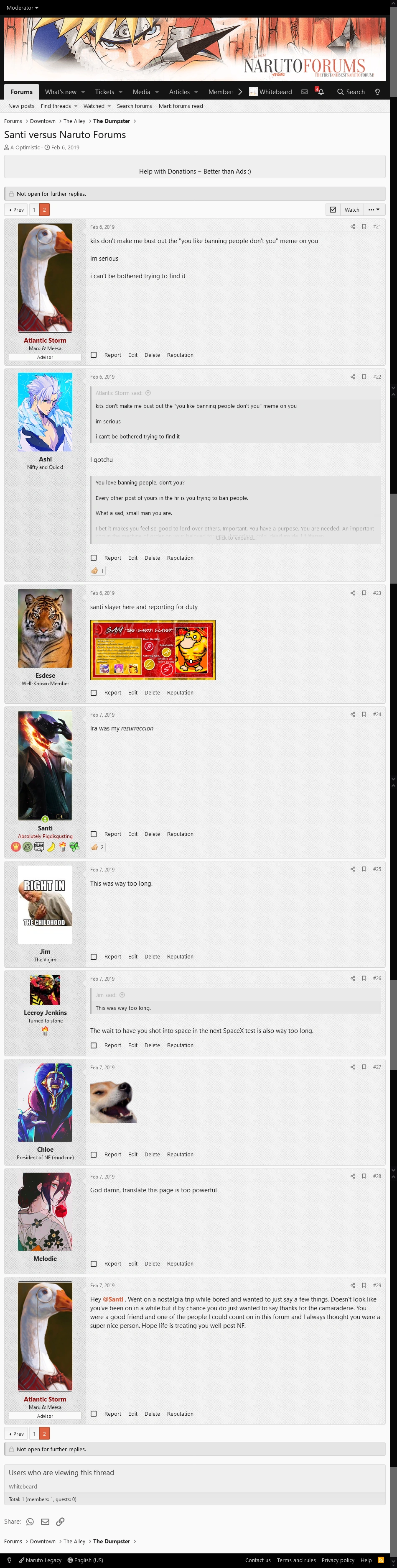 Santi versus Naruto Forums, The Alley Wiki10 abril 2025
 -
 Takt Op - Nova imagem promocional do anime original10 abril 2025
 -
![Heaven Shall Burn - Whatever It May Take [Full Album]](https://i.ytimg.com/vi/qAYOHvrhy3U/maxresdefault.jpg) Heaven Shall Burn - Whatever It May Take [Full Album]10 abril 2025
Heaven Shall Burn - Whatever It May Take [Full Album]10 abril 2025 -
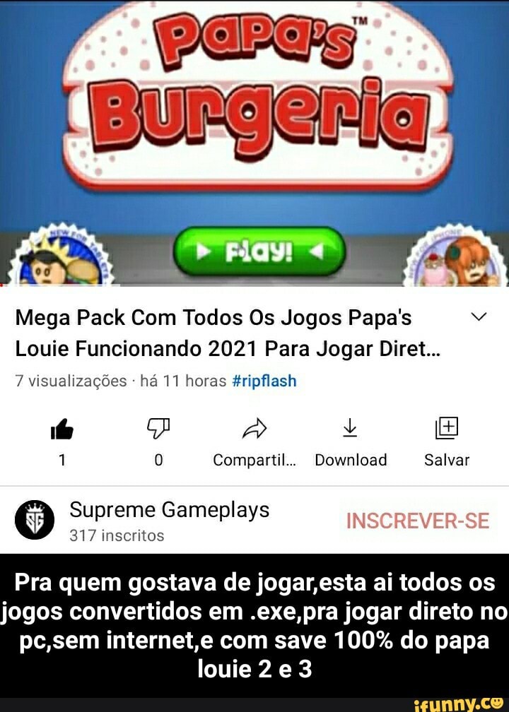 Mega Pack Com Todos Os Jogos Papa's Louie Funcionando 202% Para10 abril 2025
 -
♡ Royale High Tips and Tricks ♡ - ♡New Campus♡ - Wattpad10 abril 2025
-
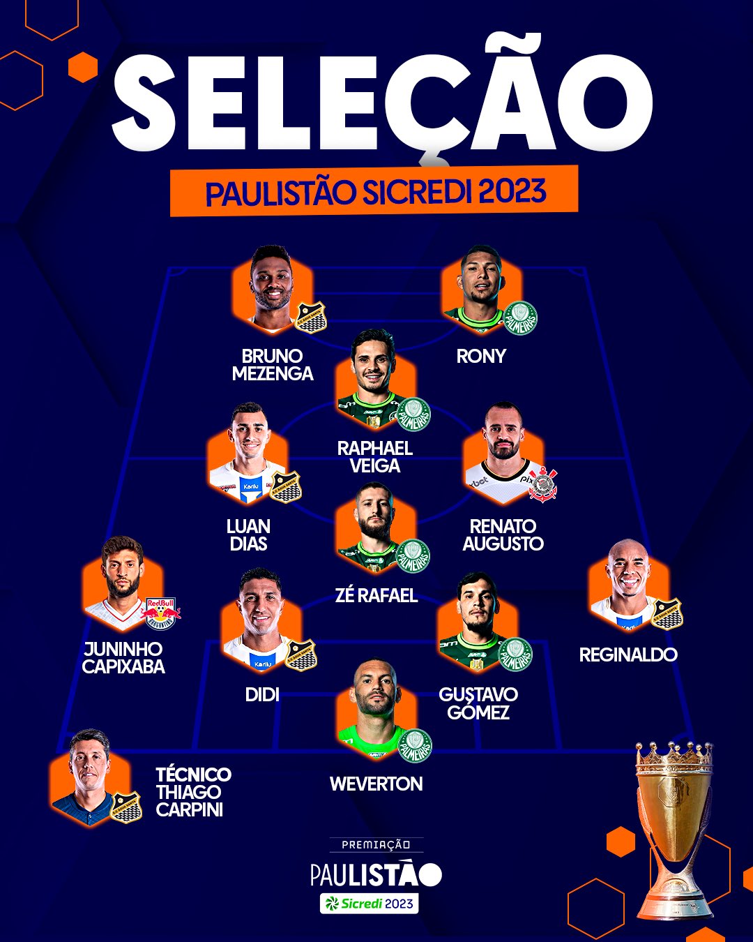 Paulistão 2023: Palmeiras tem cinco jogadores na seleção do10 abril 2025
 -
Acorda Hip Hop PDF, PDF, Música hip hop10 abril 2025

